Process Flow
The complete and detailed manufacturing process of a PCB (Printed Circuit Board) is as follows:
I. Design Phase
1.Circuit Design
●Electrical engineers use specialized software to design the circuit schematic, which shows the electrical connections between various components.
●Components such as resistors, capacitors, integrated circuits, and connectors are selected and placed on the schematic.
2.PCB Layout Design
●Based on the circuit schematic, a PCB layout designer creates a physical layout of the circuit on the PCB.
●Components are placed on the board, and traces (conductive paths) are routed to connect the components.
●Considerations such as signal integrity, power distribution, and thermal management are taken into account during layout design.
II. Material Preparation
1.Copper-Clad Laminate
●The main material for making a PCB is copper-clad laminate, which consists of a layer of copper foil bonded to a substrate material such as fiberglass-reinforced epoxy.
●Different thicknesses of copper foil and substrate materials are available depending on the application requirements.
2.Solder Mask and Silkscreen Materials
●Solder mask is a protective layer that covers the copper traces except for the areas where components are to be soldered.
●Silkscreen is used to print component labels, reference designators, and other markings on the PCB.
3.Drill Bits and Plating Chemicals
●Drill bits are needed for drilling holes in the PCB for component leads and vias (connections between different layers).
●Plating chemicals are used for plating the holes and traces with copper or other metals to improve conductivity.
III. Fabrication -
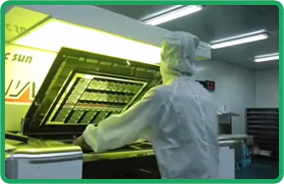
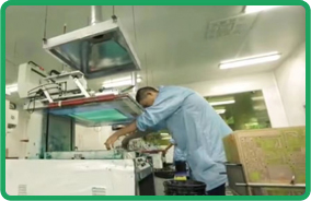
1.Imaging and Etching
●The PCB layout is transferred onto the copper-clad laminate using a photolithography process.
●A photosensitive film is applied to the copper surface, and the layout is exposed to UV light through a photomask.
●The exposed areas of the photosensitive film are developed, leaving the copper foil protected in the areas where the traces and pads are to be formed.
●The unprotected copper is then etched away using an acid or alkaline solution, leaving behind the desired circuit pattern.
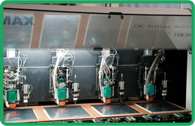
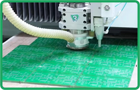
2.Drilling
●Holes are drilled in the PCB using a mechanical drill or a laser drill.
The holes can be through-holes (connecting different layers) or blind vias (connecting only two layers).
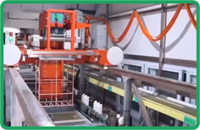
3.Plating
●The drilled holes are plated with copper to provide electrical conductivity between different layers.
●This is done by immersing the PCB in a plating bath and applying an electrical current.
●Other plating processes such as gold plating or tin plating may be used for special applications.
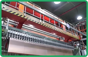
4.Soldermask Application
●A layer of solder mask is applied to the PCB using a screen printing or spraying process.
●The solder mask protects the copper traces from oxidation and prevents solder from bridging between adjacent traces.
5.Silkscreen Printing
●The silkscreen layer is printed on the PCB using a screen printing process.
●The silkscreen provides component labels, reference designators, and other markings for easy identification and assembly.
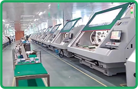
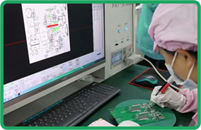
IV. Testing and Inspection
1.Electrical Testing
●The completed PCB is tested for electrical continuity and functionality using specialized testing equipment.
●In-circuit testing (ICT) and functional testing are common methods used to ensure that the PCB meets the design specifications.
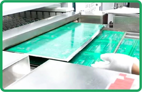
2.Visual Inspection
●The PCB is visually inspected for defects such as scratches, missing components, incorrect markings, or poor solder joints.
●Automated optical inspection (AOI) systems may also be used for high-volume production.
V. Packaging and Shipping
1.Packaging
●The PCB is packaged in a protective material such as antistatic bags or foam trays to prevent damage during shipping.
●Labels are applied to identify the PCB and provide information such as part number, revision number, and quantity.
2.Shipping
●The packaged PCB is shipped to the customer or assembly facility using a suitable shipping method.
●Care is taken to ensure that the PCB is properly protected during transit and arrives in good condition.
In conclusion, the manufacturing process of a PCB involves several steps, from design and layout to fabrication, testing, and packaging. Each step requires precision and attention to detail to ensure that the final product meets the required quality standards.
The complete process of PCBA (Printed Circuit Board Process) surface mounting is as follows:
I. PCB Preparation
1.Inspect the PCB: Check for any defects such as scratches, warping, or missing pads.
2.Clean the PCB: Remove any dust, dirt, or contaminants using a suitable cleaning agent.
II. Component Preparation
1.Receive and inspect components: Check the incoming components for correct part numbers, quantities, and packaging.
2.Bake components if necessary: Some moisture-sensitive components may need to be baked to remove moisture before assembly.
3.Tape and reel components: Components are often supplied in tape and reel packaging for automated placement.
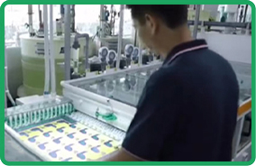
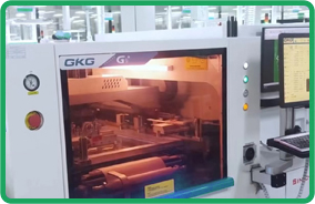
III. Solder Paste Application
1.Print solder paste: Using a stencil printer, solder paste is applied to the pads on the PCB. The stencil is aligned with the PCB, and a squeegee forces the solder paste through the openings in the stencil onto the pads.
2.Inspect solder paste: Check the solder paste deposition for correct volume, shape, and position.
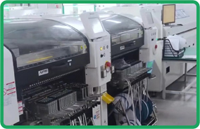
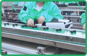
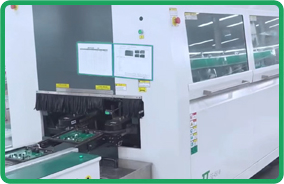
IV. Component Placement
1.Pick and place components: An automated pick and place machine picks up components from the tape and reel and places them on the PCB according to the programmed location.
2.Inspect component placement: Check the placement accuracy of the components for correct orientation, alignment, and absence of missing or misaligned components.
V. Reflow Soldering
1.Transfer PCB to reflow oven: The PCB with the placed components is transferred to a reflow oven.
2.Reflow soldering process: The reflow oven heats the PCB and components to a specific temperature profile to melt the solder paste and form solder joints. The temperature profile consists of preheating, soaking, reflowing, and cooling stages.
3.Inspect soldered joints: After reflow soldering, the soldered joints are inspected for correct shape, wetting, and absence of defects such as voids, shorts, or opens.
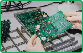
VI. Post-Soldering Inspection and Testing
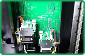
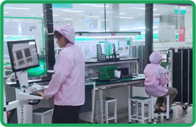
1.Visual inspection: The assembled PCB is visually inspected for any visible defects such as missing components, incorrect placement, or solder bridges.
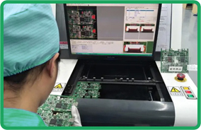
2.Automated optical inspection (AOI): AOI systems use cameras and image processing software to inspect the PCB for defects such as solder joint quality, component presence, and alignment.
3.In-circuit testing (ICT): ICT is used to test the electrical functionality of the assembled PCB by applying electrical signals and measuring responses.
4.Functional testing: Functional testing is performed to verify that the assembled PCB functions as intended according to the design specifications.
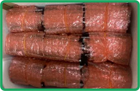
VII. Packaging and Shipping
1.Clean and protect the PCB: The assembled PCB is cleaned to remove any flux residues or contaminants. It may be coated with a protective conformal coating if required.
2.Package the PCB: The PCB is packaged in a suitable container such as an antistatic bag or box to protect it during shipping.
3.Label and document: The package is labeled with relevant information such as part number, revision number, and quantity. Documentation such as test reports and inspection records may also be included.
4.Ship the PCB: The packaged PCB is shipped to the customer or the next stage of the production process.
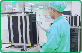
PCBA Production -
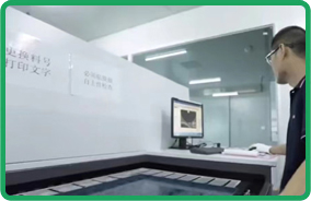
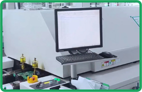
09.First Article Inspection
 Address:
  Contact: Chen Guoqiang
  Mobile: +86-13600400210
  Website: www.homaxpcb.com


 中文
中文
 Wechat
 Tel: +86-13600400210
  E-mail